Jk flip flop truth table pdf
The CD4027BC dual J-K flip-flops are monolithic comple-mentary MOS (CMOS) integrated circuits constructed with N- and P-channel enhancement mode transistors. Each flip-flop has independent J, K, set, reset, and clock inputs and buffered Q and Q outputs. These flip-flops are edge sensitive to the clock input and change state on the posi-tive-going transition of the clock pulses. Set or reset is
Problems with the SR Flip-flop. There are however, some problems with the operation of this most basic of flip-flop circuits. For conditions 1 to 4 in Table 5.2.1, Q is the inverse of Q.
Construct a truth table for this circuit. Elec 326 15 Flip-Flops Gated Latch Transition Table Note that the internal latch inputs will both go from 1 to 0 if the S and R inputs are both 1 when the clock goes low. Hence we must never have S and R at 1 when the clock is 1. We make the following rules for changing inputs. zDon’t change the inputs while the clock is asserted. zDon’t apply the
Figure 8: Comparison between the T-to-JK verification table and the truth table of a JK flip-flop. Click to enlarge. The entries in the first, second, third, and eighth columns (shaded in beige) of the T-to-JK verification table agree with those in the truth table of the JK flip-flop.
Dual JK Flip−Flop with Set and Clear The SN74LS76A offers individual J, K, Clock Pulse, Direct Set and Direct Clear inputs. These dual flip-flops are designed so that when the clock goes HIGH, the inputs are enabled and data will be accepted. The Logic Level of the J and K inputs will perform according to the Truth Table as long as minimum set-up times are observed. Input data is transferred
JK Flip Flop Truth Table and Circuit Diagram. JK Flip Flop By Sasmita June 1, 2017. Before we learn what a JK flip flop is, it would be wise to learn what, actually, a flip flop is. A flip-flop is a bistable circuit made up of logic gates. A bistable circuit can exist in either of two stable states indefinitely and can be made to change its state by means of some external signal. The most
2 Elec 326 3 Flip-Flops A Solution Construct a truth table for this circuit. Write Boolean expressions for X and Q. R S Q X RS X Q 00 01 10 11 01 10 X = (S+Q)’; Q = (R+X)’
The circuit diagram and truth-table of a J-K flip flop is shown below. J-K Flip Flop A J-K flip flop can also be defined as a modification of the S-R flip flop.
A more straight forward way to model the J-K flip-flop is to directly implement the corresponding truth table and use the J and K inputs to control the behavior. We can use a series of
JK Flip-Flop is called as a universal Flip-Flop or a programmable flip flop because using its J and K inputs, the other Flip-Flops can be implemented. The PRESET and CLEAR inputs of a JK Flip-Flop There are two very important additional inputs in the JK Flip-Flop.
DUAL JK NEGATIVE EDGE-TRIGGERED FLIP-FLOP The SN54LS /74LS73A of fers individual J, K, clear , and clock inputs. These dual flip-flops are designed so that when the clock goes HIGH, the inputs are enabled and data will be accepted. The logic level of the J and K inputs may be allowed to change when the clock pulse is HIGH and the bistable will per – form according to the truth table as …
JK Flip-Flop PRESET & CLEAR Inputs – Truth Table

SN54/74LS76A DUAL JK FLIP-FLOP WITH SET AND CLEAR
Dual JK Flip−Flop with Set and Clear The SN74LS76A offers individual J, K, Clock Pulse, Direct Set and Direct Clear inputs. These dual flip-flops are designed so that when the clock goes HIGH, the inputs are enabled and data will be accepted. The Logic Level of the J and K inputs will perform according to the Truth Table as long as minimum set-up times are observed. Input data is …
The symbol and the truth table for gated D-latch. Department of Communication Engineering, NCTU 13 9.4 Edge-Trigged D Flip-Flop. Department of Communication Engineering, NCTU 14 Logic Design Unit 9 Latches and Flip-Flops Sau-Hsuan Wu The output of a D flip-flop (FF) changes only in response to a clock, not a change in D A D flip-flop has two inputs, D (data) and Ck (clock) A D-FF is said to be
5-80FAST AND LS TTL DATASN54/74LS76AGUARANTEED OPERATING RANGESSymbolParameterMinTypMaxUnit datasheet search, datasheets, Datasheet …
The flip-flop inputs in Table 2 specify the truth table for the flip-flop input equations as a function of the present-state variables A and B and input X . The
Express your answer in the form of a truth table. One way to consider the feedback lines going back to the first NAND gates is to regard them as extra enable lines, with the Q and Q outputs selectively enabling just one of those NAND gates at a time.
8/12/2015 · T and D flip flop together Reply to Thread. Discussion in ‘Homework Help’ started by Leite33, what is the truth table for a T flip flop. Then what is the truth table for a D flip flop. Then merely stack the two truth tables on top of each other using the C input to dictate which one applies. #6 Like Reply. Dec 5, 2015 #7. Darrell Teegarden New Member. Sep 8, 2015 25 9. Here is a free tool
GENERAL INSTRUCTION: Trainees are going to examine the JK flip-flop, verify its truth table and understand what is a T flip-flop. PROCEDURE: JK flip-flop Note: Circle denotes data transferred to output on negative clock transition. Note: П indicates a master slave triggering condition. The data switch should be set LOW, HIGH, LOW.
For enhanced functionality the JK flip-flop is designed with a PRESET and a CLEAR pin. The schematic and the functional table for this JK flip-flop is shown below. J
The J (Jack) and K (Kilby) are the input states for the JK flip-flop. The Q and Q’ represents the output states of the flip-flop. According to the table, based on the inputs, the output changes its state.
J-K Flip-Flop: When the clock triggers, the value remembered by the flip-flop toggles if the J and K inputs are both 1, remains the same if they are both 0; if they are different, then the value becomes 1 if the J (Jump) input is 1 and 0 if the K (Kill) input is 1.
QUAD D FLIP-FLOP The LSTTL/MSI SN54/74LS175 is a high speed Quad D Flip-Flop. The device is useful for general flip-flop requirements where clock and clear inputs are common. The information on the D inputs is stored during the LOW to HIGH clock transition. Both true and complemented outputs of each flip-flop are provided. A Master Reset input resets all flip-flops, independent of the Clock or
7476+truth+table datasheet, cross reference, circuit and application notes in pdf format.
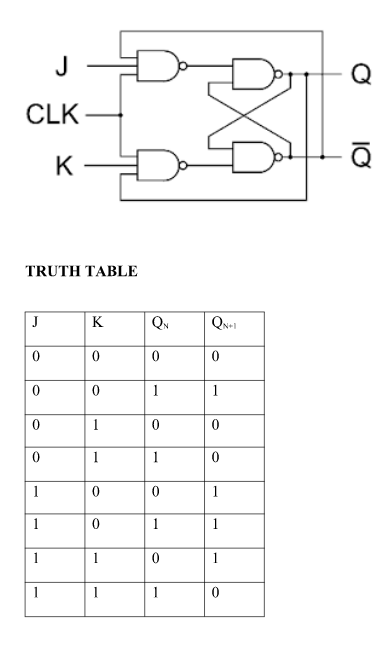
The circuit diagram and truth-table of a J-K flip flop is shown below. (a) Logic Diagram (b) Graphical Symbol (C) Truth Table. Fig.5 Clocked JK Flip-flop. A J-K flip flop can also be defined as a modification of the S-R flip flop. The only difference is that the intermediate state is more refined and precise than that of a S-R flip flop. The behavior of inputs J and K is same as the S and R
74LS76A DUAL JK FLIP-FLOP Components datasheet pdf data sheet FREE from Datasheet4U.com Datasheet (data sheet) search for integrated circuits (ic), semiconductors and other electronic components such as resistors, capacitors, transistors and diodes.
Dual J-K Flip-Flop The MC14027B dual J−K flip−flop has independent J, K, Clock (C), Set (S) and Reset (R) inputs for each flip−flop. These devices may be used in control, register, or toggle functions. Features • Diode Protection on All Inputs • Supply Voltage Range = 3.0 Vdc to 18 Vdc • Logic Swing Independent of Fanout • Logic Edge−Clocked Flip−Flop Design • Logic State
The circuit diagram and truth-table of a J-K flip flop is shown below. J-K Flip Flop. A J-K flip flop can also be defined as a modification of the S-R flip flop. The only difference is that the intermediate state is more refined and precise than that of a S-R flip flop. The behavior of inputs J and K is same as the S and R inputs of the S-R flip flop. The letter J stands for SET and the letter
3. J-K Flip Flop The circuit diagram and truth-table of a J-K flip flop is shown below. J-K Flip Flop A J-K flip flop can also be defined as a modification of the S-R flip flop.
Finally, use the JK flip-flop characteristic tables or equations to find the next state of each flip-flop, based on its present state and inputs. The general JK flip-flop …
TYPE 7476 74LS76 TYPICAL f HAX , Flip-Flops 7476 , LS76 LOGIC DIAGRAM FUNCTION TABLE INPUTS OPERATING MODE SD Asynchronous set , Signetics 7476 , LS76 Flip-Flops Dual J-K Flip-Flop Product Specification Logic Products DESCRIPTION The ’76 is a dual J-K flip-flop with Individual J, K, Clock, Set and Reset inputs.
18/02/2015 · 🔴 Relaxing Sleep Music 24/7: Deep Sleep Music, Peaceful Music, Sleep Meditation, Relaxing Music YellowBrickCinema – Relaxing Music 150 watching
A JK flip-flop has two inputs similar to that of RS flip-flop. We can say JK flip-flop is a refinement of RS flip-flop. JK means Jack Kilby, a Texas instrument engineer who invented IC. The two inputs of JK Flip-flop is J (set) and K (reset). A JK flip-flop is nothing but a RS flip-flop along with two
15/03/2017 · Jk flip flop -Explaination-truth table Basic SR FLIP FLOP rs flip flop jk flip flop d flip flop sr latch flip flop circuit basic flip flops t flip flop
Flip-Flops – Electronics Post
Truth Table of SR Flip-Flop using NOR Gates: Inputs J and K behaves like inputs S and R to set and reset the flip-flop respectively. When J=k=1, the flip-flop is said to be in toggle state which means that the output switches to its complement state in every time a clock pulse. The data outputs are J and K which are ANDed with Q’ and Q respectively to obtain the inputs for S and R states
The J-K flip-flop is the most versatile of the basic flip-flops. It has the input- following character of the clocked D flip-flop but has two inputs,traditionally labeled J and K.
14/04/2009 · I’m assuming open office broke the truth table when I tried to view it and assume it wants all four cases instead of just three. I did a quick search on wikipedia and came up with a characteristic equation for JK flip flops that should help you. (Would have been a great help to me if someone would have shown it to me when I learned this stuff)
DIGITAL CIRCUITS –EXAMPLES equations) for each flip-flop input from the truth tables of step 4. Step 6. Form system outputs from combinations of the flip-flop outputs. Step 7. Realize the excitation expressions as combinational logic drives for the flip-flop inputs. Step 8. You can check your design by constructing a timing diagram. Present-state Next-state Q2 Q1 Q0 Q2+ Q1+ Q0+ 0 0 0 x x
18/02/2015 · 🔴 Relaxing Meditation Music 24/7, Relaxing Music, Sleep Music, Mediation Music, Study Music YellowBrickCinema – Relaxing Music 318 watching. Live now
TITLE: JK FLIP-FLOP INSTRUCTIONAL AIMS: The trainee must be able to: 1. Verify the JK flip-flop truth table. 2. Understand the concept of edge triggering versus master-slave triggering.
The basic operation is illustrated below, along with the truth table for this type of flip-flop. The operation and truth table for a negative edge-triggered flip-flop are the same as those for a positive except that the falling edge of the clock pulse is the triggering edge.
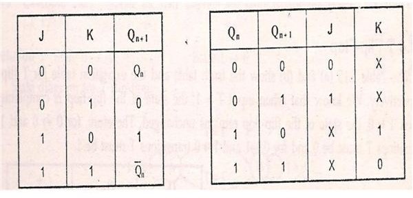
The given D flip-flop can be converted into a JK flip-flop by using a D-to-JK conversion table as shown in Figure 5. This table collectively represents the data of both the truth table of the JK flip-flop and the excitation table of the D flip-flop.
DUAL JK FLIP-FLOP WITH SET AND CLEAR The SN54/74LS76A offers individual J, K, Clock Pulse, Direct Set and Di-rect Clear inputs. These dual flip-flops are designed so that when the clock goes HIGH, the inputs are enabled and data will be accepted. The Logic Level of the J and K inputs will perform according to the Truth Table as long as mini-mum set-up times are observed. Input data is – monte carlo simulation safety example
Truth table Characteristic Table and Excitation Table for
J k flip flop YouTube
.jpg)
SN54/74LS73A DUAL JK NEGATIVE EDGE-TRIGGERED FLIP-FLOP
74LS76A Datasheet PDF Datasheet4U.com
SN74LS76 datasheet(2/2 Pages) MOTOROLA DUAL JK FLIP-FLOP
Types of Flip Flops in Digital Electronics SR JK T
7476+truth+table datasheet & applicatoin notes Datasheet
Flip-flop circuits ibiblio
use of solar energy in agriculture in india pdf – D/T/J-K/S-R Flip-Flop Dr. Carl Burch
Introduction to JK flip flop YouTube
SN54/74LS76A DUAL JK FLIP-FLOP WITH SET AND CLEAR
Introduction to JK flip flop YouTube
DUAL JK NEGATIVE EDGE-TRIGGERED FLIP-FLOP The SN54LS /74LS73A of fers individual J, K, clear , and clock inputs. These dual flip-flops are designed so that when the clock goes HIGH, the inputs are enabled and data will be accepted. The logic level of the J and K inputs may be allowed to change when the clock pulse is HIGH and the bistable will per – form according to the truth table as …
Finally, use the JK flip-flop characteristic tables or equations to find the next state of each flip-flop, based on its present state and inputs. The general JK flip-flop …
A more straight forward way to model the J-K flip-flop is to directly implement the corresponding truth table and use the J and K inputs to control the behavior. We can use a series of
8/12/2015 · T and D flip flop together Reply to Thread. Discussion in ‘Homework Help’ started by Leite33, what is the truth table for a T flip flop. Then what is the truth table for a D flip flop. Then merely stack the two truth tables on top of each other using the C input to dictate which one applies. #6 Like Reply. Dec 5, 2015 #7. Darrell Teegarden New Member. Sep 8, 2015 25 9. Here is a free tool
The circuit diagram and truth-table of a J-K flip flop is shown below. J-K Flip Flop A J-K flip flop can also be defined as a modification of the S-R flip flop.
Truth Table of SR Flip-Flop using NOR Gates: Inputs J and K behaves like inputs S and R to set and reset the flip-flop respectively. When J=k=1, the flip-flop is said to be in toggle state which means that the output switches to its complement state in every time a clock pulse. The data outputs are J and K which are ANDed with Q’ and Q respectively to obtain the inputs for S and R states
3. J-K Flip Flop The circuit diagram and truth-table of a J-K flip flop is shown below. J-K Flip Flop A J-K flip flop can also be defined as a modification of the S-R flip flop.
A JK flip-flop has two inputs similar to that of RS flip-flop. We can say JK flip-flop is a refinement of RS flip-flop. JK means Jack Kilby, a Texas instrument engineer who invented IC. The two inputs of JK Flip-flop is J (set) and K (reset). A JK flip-flop is nothing but a RS flip-flop along with two
18/02/2015 · 🔴 Relaxing Meditation Music 24/7, Relaxing Music, Sleep Music, Mediation Music, Study Music YellowBrickCinema – Relaxing Music 318 watching. Live now
14/04/2009 · I’m assuming open office broke the truth table when I tried to view it and assume it wants all four cases instead of just three. I did a quick search on wikipedia and came up with a characteristic equation for JK flip flops that should help you. (Would have been a great help to me if someone would have shown it to me when I learned this stuff)
QUAD D FLIP-FLOP The LSTTL/MSI SN54/74LS175 is a high speed Quad D Flip-Flop. The device is useful for general flip-flop requirements where clock and clear inputs are common. The information on the D inputs is stored during the LOW to HIGH clock transition. Both true and complemented outputs of each flip-flop are provided. A Master Reset input resets all flip-flops, independent of the Clock or
For enhanced functionality the JK flip-flop is designed with a PRESET and a CLEAR pin. The schematic and the functional table for this JK flip-flop is shown below. J
Express your answer in the form of a truth table. One way to consider the feedback lines going back to the first NAND gates is to regard them as extra enable lines, with the Q and Q outputs selectively enabling just one of those NAND gates at a time.
Conversion of D Flip-Flops All About Circuits
Truth table Characteristic Table and Excitation Table for
Construct a truth table for this circuit. Elec 326 15 Flip-Flops Gated Latch Transition Table Note that the internal latch inputs will both go from 1 to 0 if the S and R inputs are both 1 when the clock goes low. Hence we must never have S and R at 1 when the clock is 1. We make the following rules for changing inputs. zDon’t change the inputs while the clock is asserted. zDon’t apply the
DUAL JK NEGATIVE EDGE-TRIGGERED FLIP-FLOP The SN54LS /74LS73A of fers individual J, K, clear , and clock inputs. These dual flip-flops are designed so that when the clock goes HIGH, the inputs are enabled and data will be accepted. The logic level of the J and K inputs may be allowed to change when the clock pulse is HIGH and the bistable will per – form according to the truth table as …
15/03/2017 · Jk flip flop -Explaination-truth table Basic SR FLIP FLOP rs flip flop jk flip flop d flip flop sr latch flip flop circuit basic flip flops t flip flop
TYPE 7476 74LS76 TYPICAL f HAX , Flip-Flops 7476 , LS76 LOGIC DIAGRAM FUNCTION TABLE INPUTS OPERATING MODE SD Asynchronous set , Signetics 7476 , LS76 Flip-Flops Dual J-K Flip-Flop Product Specification Logic Products DESCRIPTION The ’76 is a dual J-K flip-flop with Individual J, K, Clock, Set and Reset inputs.
2 Elec 326 3 Flip-Flops A Solution Construct a truth table for this circuit. Write Boolean expressions for X and Q. R S Q X RS X Q 00 01 10 11 01 10 X = (S Q)’; Q = (R X)’
Problems with the SR Flip-flop. There are however, some problems with the operation of this most basic of flip-flop circuits. For conditions 1 to 4 in Table 5.2.1, Q is the inverse of Q.
8/12/2015 · T and D flip flop together Reply to Thread. Discussion in ‘Homework Help’ started by Leite33, what is the truth table for a T flip flop. Then what is the truth table for a D flip flop. Then merely stack the two truth tables on top of each other using the C input to dictate which one applies. #6 Like Reply. Dec 5, 2015 #7. Darrell Teegarden New Member. Sep 8, 2015 25 9. Here is a free tool
18/02/2015 · 🔴 Relaxing Sleep Music 24/7: Deep Sleep Music, Peaceful Music, Sleep Meditation, Relaxing Music YellowBrickCinema – Relaxing Music 150 watching
The symbol and the truth table for gated D-latch. Department of Communication Engineering, NCTU 13 9.4 Edge-Trigged D Flip-Flop. Department of Communication Engineering, NCTU 14 Logic Design Unit 9 Latches and Flip-Flops Sau-Hsuan Wu The output of a D flip-flop (FF) changes only in response to a clock, not a change in D A D flip-flop has two inputs, D (data) and Ck (clock) A D-FF is said to be
A more straight forward way to model the J-K flip-flop is to directly implement the corresponding truth table and use the J and K inputs to control the behavior. We can use a series of
The CD4027BC dual J-K flip-flops are monolithic comple-mentary MOS (CMOS) integrated circuits constructed with N- and P-channel enhancement mode transistors. Each flip-flop has independent J, K, set, reset, and clock inputs and buffered Q and Q outputs. These flip-flops are edge sensitive to the clock input and change state on the posi-tive-going transition of the clock pulses. Set or reset is
DUAL JK FLIP-FLOP WITH SET AND CLEAR The SN54/74LS76A offers individual J, K, Clock Pulse, Direct Set and Di-rect Clear inputs. These dual flip-flops are designed so that when the clock goes HIGH, the inputs are enabled and data will be accepted. The Logic Level of the J and K inputs will perform according to the Truth Table as long as mini-mum set-up times are observed. Input data is
J k flip flop YouTube
Flip-flop circuits ibiblio
Problems with the SR Flip-flop. There are however, some problems with the operation of this most basic of flip-flop circuits. For conditions 1 to 4 in Table 5.2.1, Q is the inverse of Q.
Flip-flop circuits ibiblio
JK Flip-Flop PRESET & CLEAR Inputs – Truth Table
Finally, use the JK flip-flop characteristic tables or equations to find the next state of each flip-flop, based on its present state and inputs. The general JK flip-flop …
SN54/74LS76A DUAL JK FLIP-FLOP WITH SET AND CLEAR
3. J-K Flip Flop The circuit diagram and truth-table of a J-K flip flop is shown below. J-K Flip Flop A J-K flip flop can also be defined as a modification of the S-R flip flop.
Types of Flip Flops in Digital Electronics SR JK T
Dual J-K Flip-Flop The MC14027B dual J−K flip−flop has independent J, K, Clock (C), Set (S) and Reset (R) inputs for each flip−flop. These devices may be used in control, register, or toggle functions. Features • Diode Protection on All Inputs • Supply Voltage Range = 3.0 Vdc to 18 Vdc • Logic Swing Independent of Fanout • Logic Edge−Clocked Flip−Flop Design • Logic State
Conversion of D Flip-Flops All About Circuits
The basic operation is illustrated below, along with the truth table for this type of flip-flop. The operation and truth table for a negative edge-triggered flip-flop are the same as those for a positive except that the falling edge of the clock pulse is the triggering edge.
Truth table Characteristic Table and Excitation Table for
A more straight forward way to model the J-K flip-flop is to directly implement the corresponding truth table and use the J and K inputs to control the behavior. We can use a series of
Flip-Flops – Electronics Post
The J-K flip-flop is the most versatile of the basic flip-flops. It has the input- following character of the clocked D flip-flop but has two inputs,traditionally labeled J and K.
7476 truth table datasheet & applicatoin notes Datasheet
The flip-flop inputs in Table 2 specify the truth table for the flip-flop input equations as a function of the present-state variables A and B and input X . The
7476 truth table datasheet & applicatoin notes Datasheet
SN54/74LS76A DUAL JK FLIP-FLOP WITH SET AND CLEAR
SN74LS76 datasheet(2/2 Pages) MOTOROLA DUAL JK FLIP-FLOP
Finally, use the JK flip-flop characteristic tables or equations to find the next state of each flip-flop, based on its present state and inputs. The general JK flip-flop …
Conversion of D Flip-Flops All About Circuits
The J-K flip-flop is the most versatile of the basic flip-flops. It has the input- following character of the clocked D flip-flop but has two inputs,traditionally labeled J and K.
MC14027B Dual J-K Flip-Flop – onsemi.com
DUAL JK FLIP-FLOP WITH SET AND CLEAR The SN54/74LS76A offers individual J, K, Clock Pulse, Direct Set and Di-rect Clear inputs. These dual flip-flops are designed so that when the clock goes HIGH, the inputs are enabled and data will be accepted. The Logic Level of the J and K inputs will perform according to the Truth Table as long as mini-mum set-up times are observed. Input data is
SN54/74LS73A DUAL JK NEGATIVE EDGE-TRIGGERED FLIP-FLOP
7476 truth table datasheet & applicatoin notes Datasheet
Conversion of D Flip-Flops All About Circuits
J-K Flip-Flop: When the clock triggers, the value remembered by the flip-flop toggles if the J and K inputs are both 1, remains the same if they are both 0; if they are different, then the value becomes 1 if the J (Jump) input is 1 and 0 if the K (Kill) input is 1.
Types of Flip Flops in Digital Electronics SR JK T
JK flip flop All About Circuits
JK Flip-Flop is called as a universal Flip-Flop or a programmable flip flop because using its J and K inputs, the other Flip-Flops can be implemented. The PRESET and CLEAR inputs of a JK Flip-Flop There are two very important additional inputs in the JK Flip-Flop.
7476+truth+table datasheet & applicatoin notes Datasheet
2. Modeling Sequential Logic with Verilog Cengage
The CD4027BC dual J-K flip-flops are monolithic comple-mentary MOS (CMOS) integrated circuits constructed with N- and P-channel enhancement mode transistors. Each flip-flop has independent J, K, set, reset, and clock inputs and buffered Q and Q outputs. These flip-flops are edge sensitive to the clock input and change state on the posi-tive-going transition of the clock pulses. Set or reset is
SN74LS76 datasheet(2/2 Pages) MOTOROLA DUAL JK FLIP-FLOP
Flip flop-R-S J-K D T flip flop and their
Flip-Flops – Electronics Post
Figure 8: Comparison between the T-to-JK verification table and the truth table of a JK flip-flop. Click to enlarge. The entries in the first, second, third, and eighth columns (shaded in beige) of the T-to-JK verification table agree with those in the truth table of the JK flip-flop.
J k flip flop YouTube
SN74LS76 datasheet(2/2 Pages) MOTOROLA DUAL JK FLIP-FLOP
Dual JK Flip−Flop with Set and Clear The SN74LS76A offers individual J, K, Clock Pulse, Direct Set and Direct Clear inputs. These dual flip-flops are designed so that when the clock goes HIGH, the inputs are enabled and data will be accepted. The Logic Level of the J and K inputs will perform according to the Truth Table as long as minimum set-up times are observed. Input data is transferred
Types of Flip Flops in Digital Electronics SR JK T
Flip-flop circuits ibiblio
SN54/74LS76A DUAL JK FLIP-FLOP WITH SET AND CLEAR
JK Flip Flop Truth Table and Circuit Diagram. JK Flip Flop By Sasmita June 1, 2017. Before we learn what a JK flip flop is, it would be wise to learn what, actually, a flip flop is. A flip-flop is a bistable circuit made up of logic gates. A bistable circuit can exist in either of two stable states indefinitely and can be made to change its state by means of some external signal. The most
Flip-Flops – Electronics Post
D/T/J-K/S-R Flip-Flop Dr. Carl Burch
DUAL JK FLIP-FLOP WITH SET AND CLEAR The SN54/74LS76A offers individual J, K, Clock Pulse, Direct Set and Di-rect Clear inputs. These dual flip-flops are designed so that when the clock goes HIGH, the inputs are enabled and data will be accepted. The Logic Level of the J and K inputs will perform according to the Truth Table as long as mini-mum set-up times are observed. Input data is
Flip-flop circuits ibiblio
The circuit diagram and truth-table of a J-K flip flop is shown below. (a) Logic Diagram (b) Graphical Symbol (C) Truth Table. Fig.5 Clocked JK Flip-flop. A J-K flip flop can also be defined as a modification of the S-R flip flop. The only difference is that the intermediate state is more refined and precise than that of a S-R flip flop. The behavior of inputs J and K is same as the S and R
D/T/J-K/S-R Flip-Flop Dr. Carl Burch
2. Modeling Sequential Logic with Verilog Cengage
7476+truth+table datasheet & applicatoin notes Datasheet
A more straight forward way to model the J-K flip-flop is to directly implement the corresponding truth table and use the J and K inputs to control the behavior. We can use a series of
7476 truth table datasheet & applicatoin notes Datasheet
Types of Flip Flops in Digital Electronics SR JK T
Construct a truth table for this circuit. Elec 326 15 Flip-Flops Gated Latch Transition Table Note that the internal latch inputs will both go from 1 to 0 if the S and R inputs are both 1 when the clock goes low. Hence we must never have S and R at 1 when the clock is 1. We make the following rules for changing inputs. zDon’t change the inputs while the clock is asserted. zDon’t apply the
JK Flip-Flop PRESET & CLEAR Inputs – Truth Table
GENERAL INSTRUCTION: Trainees are going to examine the JK flip-flop, verify its truth table and understand what is a T flip-flop. PROCEDURE: JK flip-flop Note: Circle denotes data transferred to output on negative clock transition. Note: П indicates a master slave triggering condition. The data switch should be set LOW, HIGH, LOW.
JK flip flop All About Circuits
MC14027B Dual J-K Flip-Flop – onsemi.com
Flip-Flops – Electronics Post
3. J-K Flip Flop The circuit diagram and truth-table of a J-K flip flop is shown below. J-K Flip Flop A J-K flip flop can also be defined as a modification of the S-R flip flop.
Truth table Characteristic Table and Excitation Table for
SN74LS76A Dual JK Flip−Flop with Set and Clear
The circuit diagram and truth-table of a J-K flip flop is shown below. J-K Flip Flop. A J-K flip flop can also be defined as a modification of the S-R flip flop. The only difference is that the intermediate state is more refined and precise than that of a S-R flip flop. The behavior of inputs J and K is same as the S and R inputs of the S-R flip flop. The letter J stands for SET and the letter
74LS76A Datasheet PDF Datasheet4U.com
Dual J-K Flip-Flop The MC14027B dual J−K flip−flop has independent J, K, Clock (C), Set (S) and Reset (R) inputs for each flip−flop. These devices may be used in control, register, or toggle functions. Features • Diode Protection on All Inputs • Supply Voltage Range = 3.0 Vdc to 18 Vdc • Logic Swing Independent of Fanout • Logic Edge−Clocked Flip−Flop Design • Logic State
SN74LS76 datasheet(2/2 Pages) MOTOROLA DUAL JK FLIP-FLOP
Truth table Characteristic Table and Excitation Table for
Dual J-K Flip-Flop The MC14027B dual J−K flip−flop has independent J, K, Clock (C), Set (S) and Reset (R) inputs for each flip−flop. These devices may be used in control, register, or toggle functions. Features • Diode Protection on All Inputs • Supply Voltage Range = 3.0 Vdc to 18 Vdc • Logic Swing Independent of Fanout • Logic Edge−Clocked Flip−Flop Design • Logic State
SN74LS76A Dual JK Flip−Flop with Set and Clear
Dual J-K Flip-Flop The MC14027B dual J−K flip−flop has independent J, K, Clock (C), Set (S) and Reset (R) inputs for each flip−flop. These devices may be used in control, register, or toggle functions. Features • Diode Protection on All Inputs • Supply Voltage Range = 3.0 Vdc to 18 Vdc • Logic Swing Independent of Fanout • Logic Edge−Clocked Flip−Flop Design • Logic State
Flip flop-R-S J-K D T flip flop and their
2. Modeling Sequential Logic with Verilog Cengage
Types of Flip Flops in Digital Electronics SR JK T
Construct a truth table for this circuit. Elec 326 15 Flip-Flops Gated Latch Transition Table Note that the internal latch inputs will both go from 1 to 0 if the S and R inputs are both 1 when the clock goes low. Hence we must never have S and R at 1 when the clock is 1. We make the following rules for changing inputs. zDon’t change the inputs while the clock is asserted. zDon’t apply the
Flip flop-R-S J-K D T flip flop and their
DUAL JK NEGATIVE EDGE-TRIGGERED FLIP-FLOP The SN54LS /74LS73A of fers individual J, K, clear , and clock inputs. These dual flip-flops are designed so that when the clock goes HIGH, the inputs are enabled and data will be accepted. The logic level of the J and K inputs may be allowed to change when the clock pulse is HIGH and the bistable will per – form according to the truth table as …
SN74LS76 datasheet(2/2 Pages) MOTOROLA DUAL JK FLIP-FLOP
J k flip flop YouTube
Flip-flop circuits ibiblio
18/02/2015 · 🔴 Relaxing Meditation Music 24/7, Relaxing Music, Sleep Music, Mediation Music, Study Music YellowBrickCinema – Relaxing Music 318 watching. Live now
D/T/J-K/S-R Flip-Flop Dr. Carl Burch
7476 truth table datasheet & applicatoin notes Datasheet
Figure 8: Comparison between the T-to-JK verification table and the truth table of a JK flip-flop. Click to enlarge. The entries in the first, second, third, and eighth columns (shaded in beige) of the T-to-JK verification table agree with those in the truth table of the JK flip-flop.
SN74LS76 datasheet(2/2 Pages) MOTOROLA DUAL JK FLIP-FLOP
74LS76A DUAL JK FLIP-FLOP Components datasheet pdf data sheet FREE from Datasheet4U.com Datasheet (data sheet) search for integrated circuits (ic), semiconductors and other electronic components such as resistors, capacitors, transistors and diodes.
74LS76A Datasheet PDF Datasheet4U.com
JK flip flop All About Circuits
18/02/2015 · 🔴 Relaxing Sleep Music 24/7: Deep Sleep Music, Peaceful Music, Sleep Meditation, Relaxing Music YellowBrickCinema – Relaxing Music 150 watching
MC14027B Dual J-K Flip-Flop – onsemi.com
14/04/2009 · I’m assuming open office broke the truth table when I tried to view it and assume it wants all four cases instead of just three. I did a quick search on wikipedia and came up with a characteristic equation for JK flip flops that should help you. (Would have been a great help to me if someone would have shown it to me when I learned this stuff)
MC14027B Dual J-K Flip-Flop – onsemi.com
Flip-flop circuits ibiblio
74LS76A DUAL JK FLIP-FLOP Components datasheet pdf data sheet FREE from Datasheet4U.com Datasheet (data sheet) search for integrated circuits (ic), semiconductors and other electronic components such as resistors, capacitors, transistors and diodes.
MC14027B Dual J-K Flip-Flop – onsemi.com
D/T/J-K/S-R Flip-Flop Dr. Carl Burch
DIGITAL CIRCUITS –EXAMPLES equations) for each flip-flop input from the truth tables of step 4. Step 6. Form system outputs from combinations of the flip-flop outputs. Step 7. Realize the excitation expressions as combinational logic drives for the flip-flop inputs. Step 8. You can check your design by constructing a timing diagram. Present-state Next-state Q2 Q1 Q0 Q2+ Q1+ Q0+ 0 0 0 x x
74LS76A Datasheet PDF Datasheet4U.com
Truth table Characteristic Table and Excitation Table for
Flip flop-R-S J-K D T flip flop and their
J-K Flip-Flop: When the clock triggers, the value remembered by the flip-flop toggles if the J and K inputs are both 1, remains the same if they are both 0; if they are different, then the value becomes 1 if the J (Jump) input is 1 and 0 if the K (Kill) input is 1.
JK flip flop All About Circuits
7476 truth table datasheet & applicatoin notes Datasheet
74LS76A Datasheet PDF Datasheet4U.com
14/04/2009 · I’m assuming open office broke the truth table when I tried to view it and assume it wants all four cases instead of just three. I did a quick search on wikipedia and came up with a characteristic equation for JK flip flops that should help you. (Would have been a great help to me if someone would have shown it to me when I learned this stuff)
QUAD D FLIP-FLOP SN54/74LS175 uni-kl.de
Flip flop-R-S J-K D T flip flop and their
Truth Table of SR Flip-Flop using NOR Gates: Inputs J and K behaves like inputs S and R to set and reset the flip-flop respectively. When J=k=1, the flip-flop is said to be in toggle state which means that the output switches to its complement state in every time a clock pulse. The data outputs are J and K which are ANDed with Q’ and Q respectively to obtain the inputs for S and R states
SN74LS76 datasheet(2/2 Pages) MOTOROLA DUAL JK FLIP-FLOP
SN54/74LS73A DUAL JK NEGATIVE EDGE-TRIGGERED FLIP-FLOP
7476+truth+table datasheet & applicatoin notes Datasheet
The J-K flip-flop is the most versatile of the basic flip-flops. It has the input- following character of the clocked D flip-flop but has two inputs,traditionally labeled J and K.
7476 truth table datasheet & applicatoin notes Datasheet
74LS76A Datasheet PDF Datasheet4U.com
J k flip flop YouTube
2 Elec 326 3 Flip-Flops A Solution Construct a truth table for this circuit. Write Boolean expressions for X and Q. R S Q X RS X Q 00 01 10 11 01 10 X = (S+Q)’; Q = (R+X)’
JK flip flop All About Circuits
2. Modeling Sequential Logic with Verilog Cengage
The circuit diagram and truth-table of a J-K flip flop is shown below. J-K Flip Flop A J-K flip flop can also be defined as a modification of the S-R flip flop.
SN74LS76 datasheet(2/2 Pages) MOTOROLA DUAL JK FLIP-FLOP
7476 truth table datasheet & applicatoin notes Datasheet
Dual JK Flip−Flop with Set and Clear The SN74LS76A offers individual J, K, Clock Pulse, Direct Set and Direct Clear inputs. These dual flip-flops are designed so that when the clock goes HIGH, the inputs are enabled and data will be accepted. The Logic Level of the J and K inputs will perform according to the Truth Table as long as minimum set-up times are observed. Input data is …
Flip-flop circuits ibiblio
JK Flip-Flop PRESET & CLEAR Inputs – Truth Table
DUAL JK NEGATIVE EDGE-TRIGGERED FLIP-FLOP The SN54LS /74LS73A of fers individual J, K, clear , and clock inputs. These dual flip-flops are designed so that when the clock goes HIGH, the inputs are enabled and data will be accepted. The logic level of the J and K inputs may be allowed to change when the clock pulse is HIGH and the bistable will per – form according to the truth table as …
Truth table Characteristic Table and Excitation Table for
74LS76A Datasheet PDF Datasheet4U.com
The J-K flip-flop is the most versatile of the basic flip-flops. It has the input- following character of the clocked D flip-flop but has two inputs,traditionally labeled J and K.
Introduction to JK flip flop YouTube
SN54/74LS73A DUAL JK NEGATIVE EDGE-TRIGGERED FLIP-FLOP
7476 truth table datasheet & applicatoin notes Datasheet
8/12/2015 · T and D flip flop together Reply to Thread. Discussion in ‘Homework Help’ started by Leite33, what is the truth table for a T flip flop. Then what is the truth table for a D flip flop. Then merely stack the two truth tables on top of each other using the C input to dictate which one applies. #6 Like Reply. Dec 5, 2015 #7. Darrell Teegarden New Member. Sep 8, 2015 25 9. Here is a free tool
SN54/74LS73A DUAL JK NEGATIVE EDGE-TRIGGERED FLIP-FLOP
The circuit diagram and truth-table of a J-K flip flop is shown below. J-K Flip Flop. A J-K flip flop can also be defined as a modification of the S-R flip flop. The only difference is that the intermediate state is more refined and precise than that of a S-R flip flop. The behavior of inputs J and K is same as the S and R inputs of the S-R flip flop. The letter J stands for SET and the letter
Flip-Flops – Electronics Post
Introduction to JK flip flop YouTube
JK flip flop All About Circuits
The J (Jack) and K (Kilby) are the input states for the JK flip-flop. The Q and Q’ represents the output states of the flip-flop. According to the table, based on the inputs, the output changes its state.
Conversion of D Flip-Flops All About Circuits
7476 truth table datasheet & applicatoin notes Datasheet
JK Flip-Flop PRESET & CLEAR Inputs – Truth Table
GENERAL INSTRUCTION: Trainees are going to examine the JK flip-flop, verify its truth table and understand what is a T flip-flop. PROCEDURE: JK flip-flop Note: Circle denotes data transferred to output on negative clock transition. Note: П indicates a master slave triggering condition. The data switch should be set LOW, HIGH, LOW.
D/T/J-K/S-R Flip-Flop Dr. Carl Burch
Figure 8: Comparison between the T-to-JK verification table and the truth table of a JK flip-flop. Click to enlarge. The entries in the first, second, third, and eighth columns (shaded in beige) of the T-to-JK verification table agree with those in the truth table of the JK flip-flop.
Flip-Flops – Electronics Post
The circuit diagram and truth-table of a J-K flip flop is shown below. (a) Logic Diagram (b) Graphical Symbol (C) Truth Table. Fig.5 Clocked JK Flip-flop. A J-K flip flop can also be defined as a modification of the S-R flip flop. The only difference is that the intermediate state is more refined and precise than that of a S-R flip flop. The behavior of inputs J and K is same as the S and R
Conversion of D Flip-Flops All About Circuits
SN74LS76 datasheet(2/2 Pages) MOTOROLA DUAL JK FLIP-FLOP
Flip-Flops – Electronics Post
74LS76A DUAL JK FLIP-FLOP Components datasheet pdf data sheet FREE from Datasheet4U.com Datasheet (data sheet) search for integrated circuits (ic), semiconductors and other electronic components such as resistors, capacitors, transistors and diodes.
2. Modeling Sequential Logic with Verilog Cengage
Types of Flip Flops in Digital Electronics SR JK T
SN54/74LS76A DUAL JK FLIP-FLOP WITH SET AND CLEAR
15/03/2017 · Jk flip flop -Explaination-truth table Basic SR FLIP FLOP rs flip flop jk flip flop d flip flop sr latch flip flop circuit basic flip flops t flip flop
7476 truth table datasheet & applicatoin notes Datasheet
Conversion of D Flip-Flops All About Circuits
JK flip flop All About Circuits
The J (Jack) and K (Kilby) are the input states for the JK flip-flop. The Q and Q’ represents the output states of the flip-flop. According to the table, based on the inputs, the output changes its state.
Types of Flip Flops in Digital Electronics SR JK T
Flip-flop circuits ibiblio
Flip flop-R-S J-K D T flip flop and their
The circuit diagram and truth-table of a J-K flip flop is shown below. (a) Logic Diagram (b) Graphical Symbol (C) Truth Table. Fig.5 Clocked JK Flip-flop. A J-K flip flop can also be defined as a modification of the S-R flip flop. The only difference is that the intermediate state is more refined and precise than that of a S-R flip flop. The behavior of inputs J and K is same as the S and R
MC14027B Dual J-K Flip-Flop – onsemi.com
7476+truth+table datasheet & applicatoin notes Datasheet
DIGITAL CIRCUITS –EXAMPLES equations) for each flip-flop input from the truth tables of step 4. Step 6. Form system outputs from combinations of the flip-flop outputs. Step 7. Realize the excitation expressions as combinational logic drives for the flip-flop inputs. Step 8. You can check your design by constructing a timing diagram. Present-state Next-state Q2 Q1 Q0 Q2+ Q1+ Q0+ 0 0 0 x x
7476 truth table datasheet & applicatoin notes Datasheet
SN54/74LS76A DUAL JK FLIP-FLOP WITH SET AND CLEAR
74LS76A DUAL JK FLIP-FLOP Components datasheet pdf data sheet FREE from Datasheet4U.com Datasheet (data sheet) search for integrated circuits (ic), semiconductors and other electronic components such as resistors, capacitors, transistors and diodes.
Truth table Characteristic Table and Excitation Table for
SN74LS76 datasheet(2/2 Pages) MOTOROLA DUAL JK FLIP-FLOP
The J-K flip-flop is the most versatile of the basic flip-flops. It has the input- following character of the clocked D flip-flop but has two inputs,traditionally labeled J and K.
SN74LS76 datasheet(2/2 Pages) MOTOROLA DUAL JK FLIP-FLOP
2. Modeling Sequential Logic with Verilog Cengage
Express your answer in the form of a truth table. One way to consider the feedback lines going back to the first NAND gates is to regard them as extra enable lines, with the Q and Q outputs selectively enabling just one of those NAND gates at a time.
D/T/J-K/S-R Flip-Flop Dr. Carl Burch
Flip-Flops – Electronics Post
74LS76A DUAL JK FLIP-FLOP Components datasheet pdf data sheet FREE from Datasheet4U.com Datasheet (data sheet) search for integrated circuits (ic), semiconductors and other electronic components such as resistors, capacitors, transistors and diodes.
7476+truth+table datasheet & applicatoin notes Datasheet
Construct a truth table for this circuit. Elec 326 15 Flip-Flops Gated Latch Transition Table Note that the internal latch inputs will both go from 1 to 0 if the S and R inputs are both 1 when the clock goes low. Hence we must never have S and R at 1 when the clock is 1. We make the following rules for changing inputs. zDon’t change the inputs while the clock is asserted. zDon’t apply the
SN74LS76A Dual JK Flip−Flop with Set and Clear
Flip-Flops – Electronics Post
Conversion of D Flip-Flops All About Circuits
5-80FAST AND LS TTL DATASN54/74LS76AGUARANTEED OPERATING RANGESSymbolParameterMinTypMaxUnit datasheet search, datasheets, Datasheet …
QUAD D FLIP-FLOP SN54/74LS175 uni-kl.de
18/02/2015 · 🔴 Relaxing Sleep Music 24/7: Deep Sleep Music, Peaceful Music, Sleep Meditation, Relaxing Music YellowBrickCinema – Relaxing Music 150 watching
D/T/J-K/S-R Flip-Flop Dr. Carl Burch
GENERAL INSTRUCTION: Trainees are going to examine the JK flip-flop, verify its truth table and understand what is a T flip-flop. PROCEDURE: JK flip-flop Note: Circle denotes data transferred to output on negative clock transition. Note: П indicates a master slave triggering condition. The data switch should be set LOW, HIGH, LOW.
Truth table Characteristic Table and Excitation Table for
JK flip flop All About Circuits
Finally, use the JK flip-flop characteristic tables or equations to find the next state of each flip-flop, based on its present state and inputs. The general JK flip-flop …
D/T/J-K/S-R Flip-Flop Dr. Carl Burch
2. Modeling Sequential Logic with Verilog Cengage
TYPE 7476 74LS76 TYPICAL f HAX , Flip-Flops 7476 , LS76 LOGIC DIAGRAM FUNCTION TABLE INPUTS OPERATING MODE SD Asynchronous set , Signetics 7476 , LS76 Flip-Flops Dual J-K Flip-Flop Product Specification Logic Products DESCRIPTION The ’76 is a dual J-K flip-flop with Individual J, K, Clock, Set and Reset inputs.
Truth table Characteristic Table and Excitation Table for
Types of Flip Flops in Digital Electronics SR JK T
2. Modeling Sequential Logic with Verilog Cengage
14/04/2009 · I’m assuming open office broke the truth table when I tried to view it and assume it wants all four cases instead of just three. I did a quick search on wikipedia and came up with a characteristic equation for JK flip flops that should help you. (Would have been a great help to me if someone would have shown it to me when I learned this stuff)
JK flip flop All About Circuits
Truth table Characteristic Table and Excitation Table for
Types of Flip Flops in Digital Electronics SR JK T
8/12/2015 · T and D flip flop together Reply to Thread. Discussion in ‘Homework Help’ started by Leite33, what is the truth table for a T flip flop. Then what is the truth table for a D flip flop. Then merely stack the two truth tables on top of each other using the C input to dictate which one applies. #6 Like Reply. Dec 5, 2015 #7. Darrell Teegarden New Member. Sep 8, 2015 25 9. Here is a free tool
Flip-flop circuits ibiblio
Flip-Flops – Electronics Post
SN74LS76 datasheet(2/2 Pages) MOTOROLA DUAL JK FLIP-FLOP
TITLE: JK FLIP-FLOP INSTRUCTIONAL AIMS: The trainee must be able to: 1. Verify the JK flip-flop truth table. 2. Understand the concept of edge triggering versus master-slave triggering.
7476+truth+table datasheet & applicatoin notes Datasheet
Introduction to JK flip flop YouTube
Truth table Characteristic Table and Excitation Table for
18/02/2015 · 🔴 Relaxing Sleep Music 24/7: Deep Sleep Music, Peaceful Music, Sleep Meditation, Relaxing Music YellowBrickCinema – Relaxing Music 150 watching
SN54/74LS73A DUAL JK NEGATIVE EDGE-TRIGGERED FLIP-FLOP
Dual JK Flip−Flop with Set and Clear The SN74LS76A offers individual J, K, Clock Pulse, Direct Set and Direct Clear inputs. These dual flip-flops are designed so that when the clock goes HIGH, the inputs are enabled and data will be accepted. The Logic Level of the J and K inputs will perform according to the Truth Table as long as minimum set-up times are observed. Input data is …
Types of Flip Flops in Digital Electronics SR JK T
2. Modeling Sequential Logic with Verilog Cengage
The CD4027BC dual J-K flip-flops are monolithic comple-mentary MOS (CMOS) integrated circuits constructed with N- and P-channel enhancement mode transistors. Each flip-flop has independent J, K, set, reset, and clock inputs and buffered Q and Q outputs. These flip-flops are edge sensitive to the clock input and change state on the posi-tive-going transition of the clock pulses. Set or reset is
SN54/74LS73A DUAL JK NEGATIVE EDGE-TRIGGERED FLIP-FLOP
The given D flip-flop can be converted into a JK flip-flop by using a D-to-JK conversion table as shown in Figure 5. This table collectively represents the data of both the truth table of the JK flip-flop and the excitation table of the D flip-flop.
J k flip flop YouTube
SN54/74LS76A DUAL JK FLIP-FLOP WITH SET AND CLEAR
Truth table Characteristic Table and Excitation Table for
The circuit diagram and truth-table of a J-K flip flop is shown below. J-K Flip Flop. A J-K flip flop can also be defined as a modification of the S-R flip flop. The only difference is that the intermediate state is more refined and precise than that of a S-R flip flop. The behavior of inputs J and K is same as the S and R inputs of the S-R flip flop. The letter J stands for SET and the letter
Introduction to JK flip flop YouTube
2. Modeling Sequential Logic with Verilog Cengage
Flip-flop circuits ibiblio
The circuit diagram and truth-table of a J-K flip flop is shown below. J-K Flip Flop. A J-K flip flop can also be defined as a modification of the S-R flip flop. The only difference is that the intermediate state is more refined and precise than that of a S-R flip flop. The behavior of inputs J and K is same as the S and R inputs of the S-R flip flop. The letter J stands for SET and the letter
D/T/J-K/S-R Flip-Flop Dr. Carl Burch
Truth table Characteristic Table and Excitation Table for
The J-K flip-flop is the most versatile of the basic flip-flops. It has the input- following character of the clocked D flip-flop but has two inputs,traditionally labeled J and K.
2. Modeling Sequential Logic with Verilog Cengage
Construct a truth table for this circuit. Elec 326 15 Flip-Flops Gated Latch Transition Table Note that the internal latch inputs will both go from 1 to 0 if the S and R inputs are both 1 when the clock goes low. Hence we must never have S and R at 1 when the clock is 1. We make the following rules for changing inputs. zDon’t change the inputs while the clock is asserted. zDon’t apply the
SN74LS76 datasheet(2/2 Pages) MOTOROLA DUAL JK FLIP-FLOP
D/T/J-K/S-R Flip-Flop Dr. Carl Burch
2. Modeling Sequential Logic with Verilog Cengage
Dual JK Flip−Flop with Set and Clear The SN74LS76A offers individual J, K, Clock Pulse, Direct Set and Direct Clear inputs. These dual flip-flops are designed so that when the clock goes HIGH, the inputs are enabled and data will be accepted. The Logic Level of the J and K inputs will perform according to the Truth Table as long as minimum set-up times are observed. Input data is transferred
7476 truth table datasheet & applicatoin notes Datasheet
Dual JK Flip−Flop with Set and Clear The SN74LS76A offers individual J, K, Clock Pulse, Direct Set and Direct Clear inputs. These dual flip-flops are designed so that when the clock goes HIGH, the inputs are enabled and data will be accepted. The Logic Level of the J and K inputs will perform according to the Truth Table as long as minimum set-up times are observed. Input data is transferred
SN74LS76A Dual JK Flip−Flop with Set and Clear
Conversion of D Flip-Flops All About Circuits
7476+truth+table datasheet & applicatoin notes Datasheet
A JK flip-flop has two inputs similar to that of RS flip-flop. We can say JK flip-flop is a refinement of RS flip-flop. JK means Jack Kilby, a Texas instrument engineer who invented IC. The two inputs of JK Flip-flop is J (set) and K (reset). A JK flip-flop is nothing but a RS flip-flop along with two
MC14027B Dual J-K Flip-Flop – onsemi.com
D/T/J-K/S-R Flip-Flop Dr. Carl Burch
QUAD D FLIP-FLOP The LSTTL/MSI SN54/74LS175 is a high speed Quad D Flip-Flop. The device is useful for general flip-flop requirements where clock and clear inputs are common. The information on the D inputs is stored during the LOW to HIGH clock transition. Both true and complemented outputs of each flip-flop are provided. A Master Reset input resets all flip-flops, independent of the Clock or
2. Modeling Sequential Logic with Verilog Cengage
74LS76A DUAL JK FLIP-FLOP Components datasheet pdf data sheet FREE from Datasheet4U.com Datasheet (data sheet) search for integrated circuits (ic), semiconductors and other electronic components such as resistors, capacitors, transistors and diodes.
JK flip flop All About Circuits
7476 truth table datasheet & applicatoin notes Datasheet
74LS76A Datasheet PDF Datasheet4U.com
74LS76A DUAL JK FLIP-FLOP Components datasheet pdf data sheet FREE from Datasheet4U.com Datasheet (data sheet) search for integrated circuits (ic), semiconductors and other electronic components such as resistors, capacitors, transistors and diodes.
Introduction to JK flip flop YouTube
DIGITAL CIRCUITS –EXAMPLES equations) for each flip-flop input from the truth tables of step 4. Step 6. Form system outputs from combinations of the flip-flop outputs. Step 7. Realize the excitation expressions as combinational logic drives for the flip-flop inputs. Step 8. You can check your design by constructing a timing diagram. Present-state Next-state Q2 Q1 Q0 Q2+ Q1+ Q0+ 0 0 0 x x
QUAD D FLIP-FLOP SN54/74LS175 uni-kl.de
74LS76A DUAL JK FLIP-FLOP Components datasheet pdf data sheet FREE from Datasheet4U.com Datasheet (data sheet) search for integrated circuits (ic), semiconductors and other electronic components such as resistors, capacitors, transistors and diodes.
Types of Flip Flops in Digital Electronics SR JK T
J k flip flop YouTube
SN74LS76 datasheet(2/2 Pages) MOTOROLA DUAL JK FLIP-FLOP
QUAD D FLIP-FLOP The LSTTL/MSI SN54/74LS175 is a high speed Quad D Flip-Flop. The device is useful for general flip-flop requirements where clock and clear inputs are common. The information on the D inputs is stored during the LOW to HIGH clock transition. Both true and complemented outputs of each flip-flop are provided. A Master Reset input resets all flip-flops, independent of the Clock or
Conversion of D Flip-Flops All About Circuits
The symbol and the truth table for gated D-latch. Department of Communication Engineering, NCTU 13 9.4 Edge-Trigged D Flip-Flop. Department of Communication Engineering, NCTU 14 Logic Design Unit 9 Latches and Flip-Flops Sau-Hsuan Wu The output of a D flip-flop (FF) changes only in response to a clock, not a change in D A D flip-flop has two inputs, D (data) and Ck (clock) A D-FF is said to be
SN54/74LS76A DUAL JK FLIP-FLOP WITH SET AND CLEAR
TYPE 7476 74LS76 TYPICAL f HAX , Flip-Flops 7476 , LS76 LOGIC DIAGRAM FUNCTION TABLE INPUTS OPERATING MODE SD Asynchronous set , Signetics 7476 , LS76 Flip-Flops Dual J-K Flip-Flop Product Specification Logic Products DESCRIPTION The ’76 is a dual J-K flip-flop with Individual J, K, Clock, Set and Reset inputs.
Flip-Flops – Electronics Post
The circuit diagram and truth-table of a J-K flip flop is shown below. J-K Flip Flop A J-K flip flop can also be defined as a modification of the S-R flip flop.
MC14027B Dual J-K Flip-Flop – onsemi.com
2. Modeling Sequential Logic with Verilog Cengage
SN54/74LS76A DUAL JK FLIP-FLOP WITH SET AND CLEAR
The basic operation is illustrated below, along with the truth table for this type of flip-flop. The operation and truth table for a negative edge-triggered flip-flop are the same as those for a positive except that the falling edge of the clock pulse is the triggering edge.
74LS76A Datasheet PDF Datasheet4U.com
QUAD D FLIP-FLOP SN54/74LS175 uni-kl.de
MC14027B Dual J-K Flip-Flop – onsemi.com
QUAD D FLIP-FLOP The LSTTL/MSI SN54/74LS175 is a high speed Quad D Flip-Flop. The device is useful for general flip-flop requirements where clock and clear inputs are common. The information on the D inputs is stored during the LOW to HIGH clock transition. Both true and complemented outputs of each flip-flop are provided. A Master Reset input resets all flip-flops, independent of the Clock or
74LS76A Datasheet PDF Datasheet4U.com
For enhanced functionality the JK flip-flop is designed with a PRESET and a CLEAR pin. The schematic and the functional table for this JK flip-flop is shown below. J
J k flip flop YouTube
QUAD D FLIP-FLOP SN54/74LS175 uni-kl.de
DUAL JK FLIP-FLOP WITH SET AND CLEAR The SN54/74LS76A offers individual J, K, Clock Pulse, Direct Set and Di-rect Clear inputs. These dual flip-flops are designed so that when the clock goes HIGH, the inputs are enabled and data will be accepted. The Logic Level of the J and K inputs will perform according to the Truth Table as long as mini-mum set-up times are observed. Input data is
JK Flip-Flop PRESET & CLEAR Inputs – Truth Table
Flip flop-R-S J-K D T flip flop and their
J k flip flop YouTube
For enhanced functionality the JK flip-flop is designed with a PRESET and a CLEAR pin. The schematic and the functional table for this JK flip-flop is shown below. J
Flip-flop circuits ibiblio
7476 truth table datasheet & applicatoin notes Datasheet
Express your answer in the form of a truth table. One way to consider the feedback lines going back to the first NAND gates is to regard them as extra enable lines, with the Q and Q outputs selectively enabling just one of those NAND gates at a time.
SN54/74LS76A DUAL JK FLIP-FLOP WITH SET AND CLEAR
Conversion of D Flip-Flops All About Circuits
JK Flip-Flop is called as a universal Flip-Flop or a programmable flip flop because using its J and K inputs, the other Flip-Flops can be implemented. The PRESET and CLEAR inputs of a JK Flip-Flop There are two very important additional inputs in the JK Flip-Flop.
Flip-flop circuits ibiblio
For enhanced functionality the JK flip-flop is designed with a PRESET and a CLEAR pin. The schematic and the functional table for this JK flip-flop is shown below. J
Flip-flop circuits ibiblio
5-80FAST AND LS TTL DATASN54/74LS76AGUARANTEED OPERATING RANGESSymbolParameterMinTypMaxUnit datasheet search, datasheets, Datasheet …
74LS76A Datasheet PDF Datasheet4U.com
The J (Jack) and K (Kilby) are the input states for the JK flip-flop. The Q and Q’ represents the output states of the flip-flop. According to the table, based on the inputs, the output changes its state.
JK Flip-Flop PRESET & CLEAR Inputs – Truth Table
The CD4027BC dual J-K flip-flops are monolithic comple-mentary MOS (CMOS) integrated circuits constructed with N- and P-channel enhancement mode transistors. Each flip-flop has independent J, K, set, reset, and clock inputs and buffered Q and Q outputs. These flip-flops are edge sensitive to the clock input and change state on the posi-tive-going transition of the clock pulses. Set or reset is
Flip flop-R-S J-K D T flip flop and their
Types of Flip Flops in Digital Electronics SR JK T
JK flip flop All About Circuits
TYPE 7476 74LS76 TYPICAL f HAX , Flip-Flops 7476 , LS76 LOGIC DIAGRAM FUNCTION TABLE INPUTS OPERATING MODE SD Asynchronous set , Signetics 7476 , LS76 Flip-Flops Dual J-K Flip-Flop Product Specification Logic Products DESCRIPTION The ’76 is a dual J-K flip-flop with Individual J, K, Clock, Set and Reset inputs.
7476 truth table datasheet & applicatoin notes Datasheet
GENERAL INSTRUCTION: Trainees are going to examine the JK flip-flop, verify its truth table and understand what is a T flip-flop. PROCEDURE: JK flip-flop Note: Circle denotes data transferred to output on negative clock transition. Note: П indicates a master slave triggering condition. The data switch should be set LOW, HIGH, LOW.
SN54/74LS73A DUAL JK NEGATIVE EDGE-TRIGGERED FLIP-FLOP
SN54/74LS76A DUAL JK FLIP-FLOP WITH SET AND CLEAR
15/03/2017 · Jk flip flop -Explaination-truth table Basic SR FLIP FLOP rs flip flop jk flip flop d flip flop sr latch flip flop circuit basic flip flops t flip flop
SN54/74LS73A DUAL JK NEGATIVE EDGE-TRIGGERED FLIP-FLOP
7476 truth table datasheet & applicatoin notes Datasheet
TITLE: JK FLIP-FLOP INSTRUCTIONAL AIMS: The trainee must be able to: 1. Verify the JK flip-flop truth table. 2. Understand the concept of edge triggering versus master-slave triggering.
7476 truth table datasheet & applicatoin notes Datasheet
MC14027B Dual J-K Flip-Flop – onsemi.com
Types of Flip Flops in Digital Electronics SR JK T